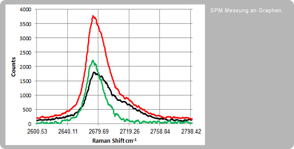
Special measurement methods in nanotechnology SPM measurements on graphs
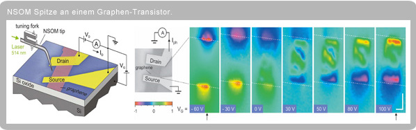
Studies on graphene, carbon nanotubes (CNTs) and functionalized carbons currently play a major role and were the subject of the last Nobel Prize in Physics awarded to A. Geim and K. Novoselov. An important tool for examining such substances is a scanning probe microscope (SPM), as manufactured by Nanonics and sold by Soliton. This allows AFM measurements to be carried out in combination with many other interesting tasks. In the work mentioned below, conductivity is studied as a function of light incidence through the NSOM tip on a graphene transistor.
The study of the interaction of matter/light/electric fields is also interesting. With a Nanonics NSOM tip with a 50 nm light exit aperture, you can, for example, illuminate a substrate and measure the electric fields generated using the Electrical Force (EFM) or Kelvin method.
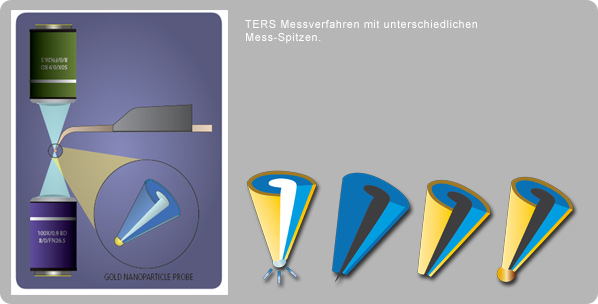
TERS measurements on graphs (Tip Enhanced Raman Scattering)
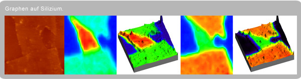
When studying graphs, it is important to know whether it is single-layer or multi-layer
The number of layers has an important influence on the physical behavior. Mounted on special substrates, this question can be glimpsed under the microscope. However, many research groups would like to combine graphene with other supports or make the question of purity and structure measurable.
TERS seems to be a new, interesting tool here, as we can show from measurements from Nanonics. While a volume of approximately 1µ x 1µ x 2µ is illuminated and measured with conventional (=far-field) Raman, with TERS the lateral spread and, above all, the penetration depth can be significantly reduced. Recently, Nanonics was able to impressively demonstrate this – as shown below