
SPM and TERS measurements on graphs
Graphene, one of the most fascinating materials of nanotechnology, is therefore the focus of numerous studies and applications. From carbon nano tubes (CNT) to functionalized carbons, graphene also offers enormous potential for research and industry. In particular, SPM measurements (scanning probe microscopy) and TERS measurements (Tip-Enhanced Raman Scattering) have established themselves as key technologies for the investigation of graphene. Furthermore, these methods provide precise insights into the material’s physical properties and structure.
SPM measurements on graphene
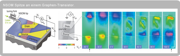
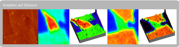
SPM measurements on graphene are among the most important analytical methods in nanotechnology. With a scanning probe microscope (SPM), such as the one from Nanonics developed and implemented by Soliton By analyzing the atomic structures and material properties of a material, detailed studies can be conducted. A SPM allows for the combination of AFM measurements (Atomic Force Microscopy) with other measurement methods. For example, the conductivity of a graphene transistor can be analyzed as a function of the light penetration through the NSOM tip (Near-Field Scanning Optical Microscopy).
Another exciting field of research is the interaction of matter, light, and electric fields. With an NSOM tip from Nanonics, which has a light exit aperture of only 50 nm, substrates can be targetedly illuminated. The electric fields generated can be measured using Electrical Force Microscopy (EFM) or the Kelvin method. This combination of methods opens up new possibilities for characterizing graphene.
TERS measurements on graphene
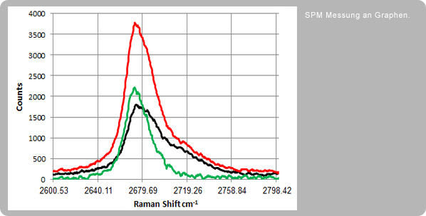
TERS measurements (Tip-Enhanced Raman Scattering) offer an innovative method for analyzing graphene, especially for determining single-layer and multi-layer structures. The number of layers has a significant impact on the material’s physical properties. While conventional Raman spectroscopy equipment illuminates larger volumes (approx. 1 µm x 1 µm x 2 µm), TERS allows for a significant reduction in the laterally illuminated area and the penetration depth. This allows for extremely precise determination of the purity, structure, and layer number of graphene.
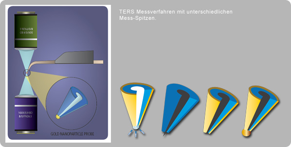
Therefore, TERS has become an indispensable tool especially for applications on special substrates or when graphene is combined with other carrier materials. Furthermore, as recently demonstrated by Nanonics, TERS enables the analysis of graphene layers with impressive accuracy. Moreover, this method is increasingly being used in research groups focused on material development and quality control.
Conclusion
SPM and TERS measurements on graphene therefore provide indispensable insights into the structure and properties of this innovative material. Technologies such as the NSOM and AFM tips from Nanonics can be used to study specific properties of graphene that are otherwise unattainable using conventional methods. Furthermore, these techniques are essential for developing new applications and materials in nanotechnology.