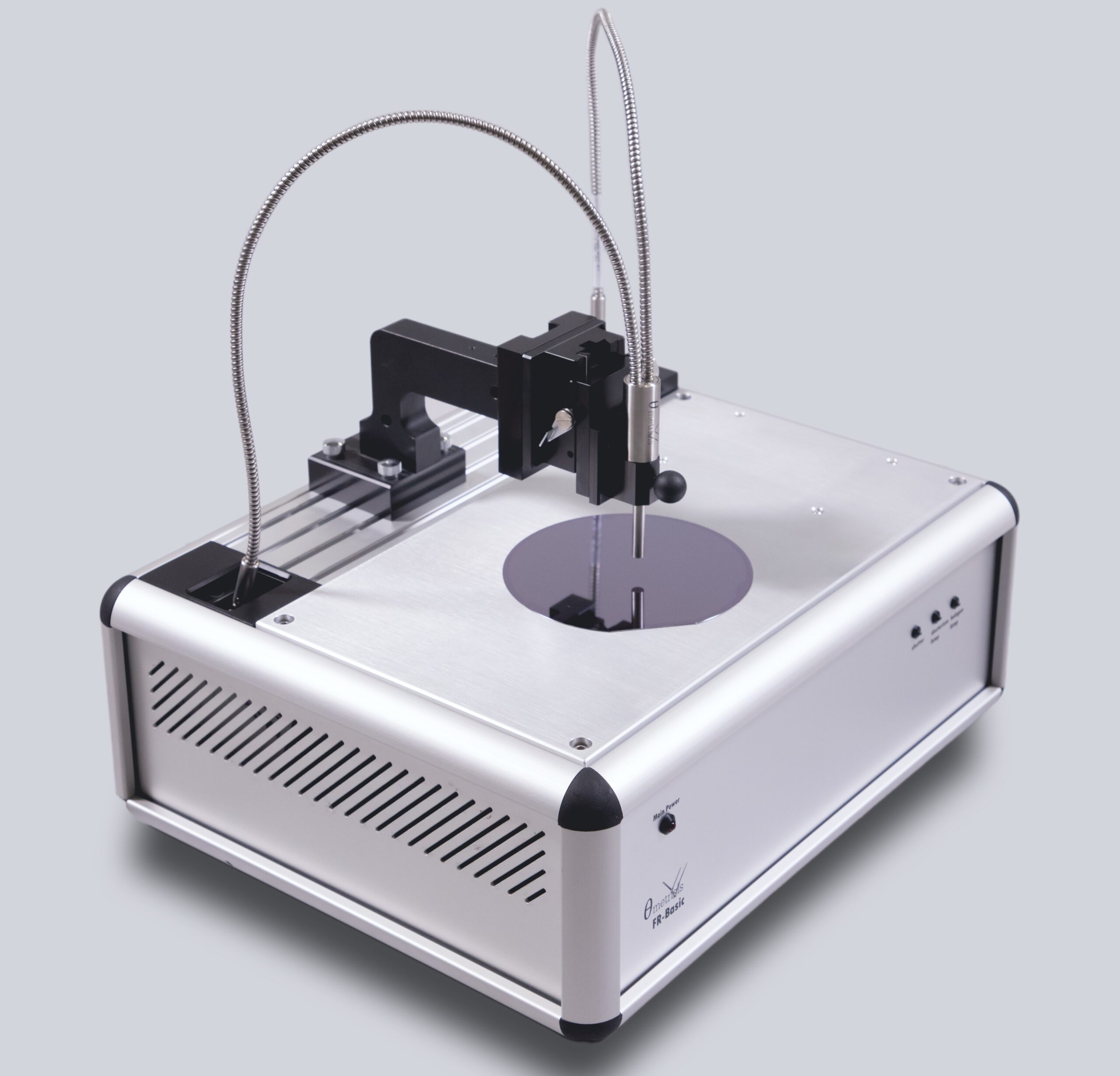
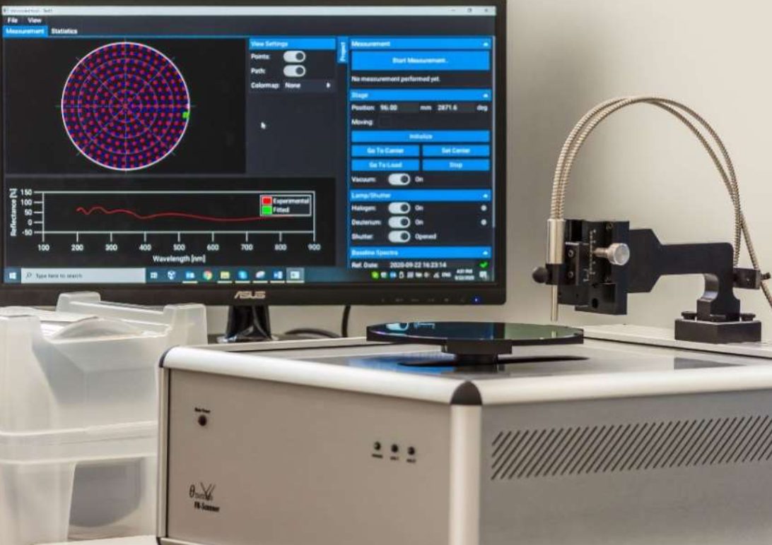


ThetaMetrisis offers a range of high-precision systems for measuring and characterizing layer thicknesses based on white light reflection spectroscopy (WLRS). Coating thickness gauges for transparent coatings measure even the smallest layers of a wide variety of materials. By using a broadband light source, a spectrometer (VIS-NIR possible) and coupling via optical fibers, you can also capture complex layer stacks and characterize their different layers.
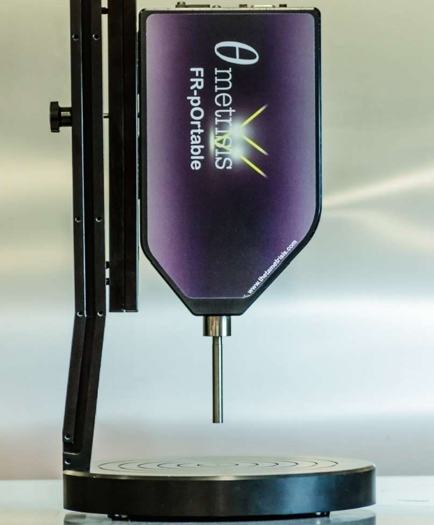
Our systems work by interfering with light rays after they are reflected from the surface of layers lying on top of each other. This interference allows you to accurately calculate the layer thickness and other relevant parameters. We offer a wide range of systems, from simple stand systems for measurements on straight surfaces to special applications. You can even measure more complex structures such as curved lenses. We use a mounting unit coupled to a fiber.
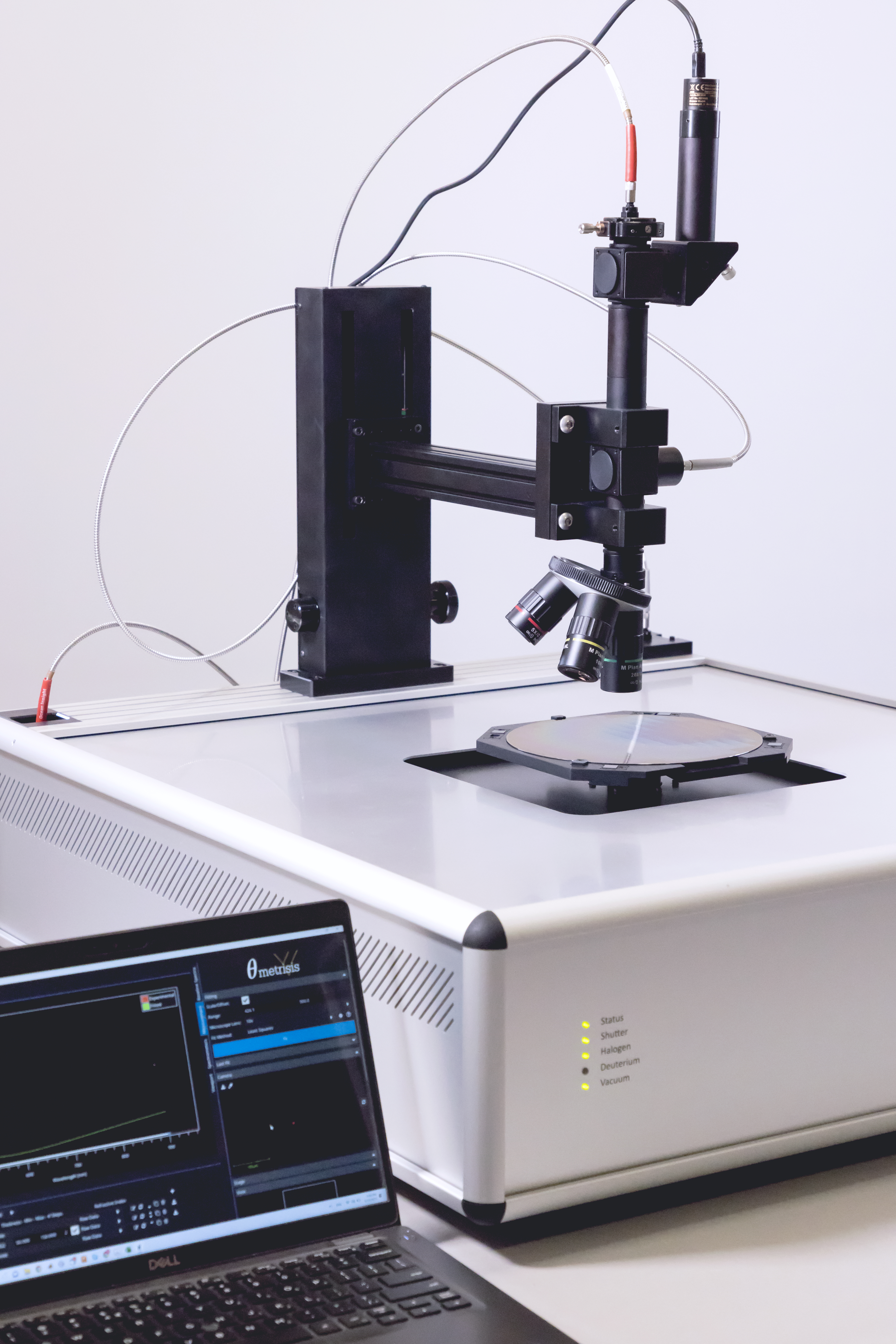
For special applications, you can also couple your coating thickness gauge for transparent layers to a microscope to precisely measure highly curved surfaces or to minimize interference factors such as roughness.
Our systems are widely used in the thickness determination of silicon layers on wafers. For example, in coating measurement on electronic parts as well as on lenses and car headlights. You benefit from fast, non-destructive and accurate characterization of thin layers and coatings on a variety of materials. With their versatility and user-friendliness, the Coating thickness gauges for transparent coatings from ThetaMetrisis ideal for use in research and development, quality control and production.
