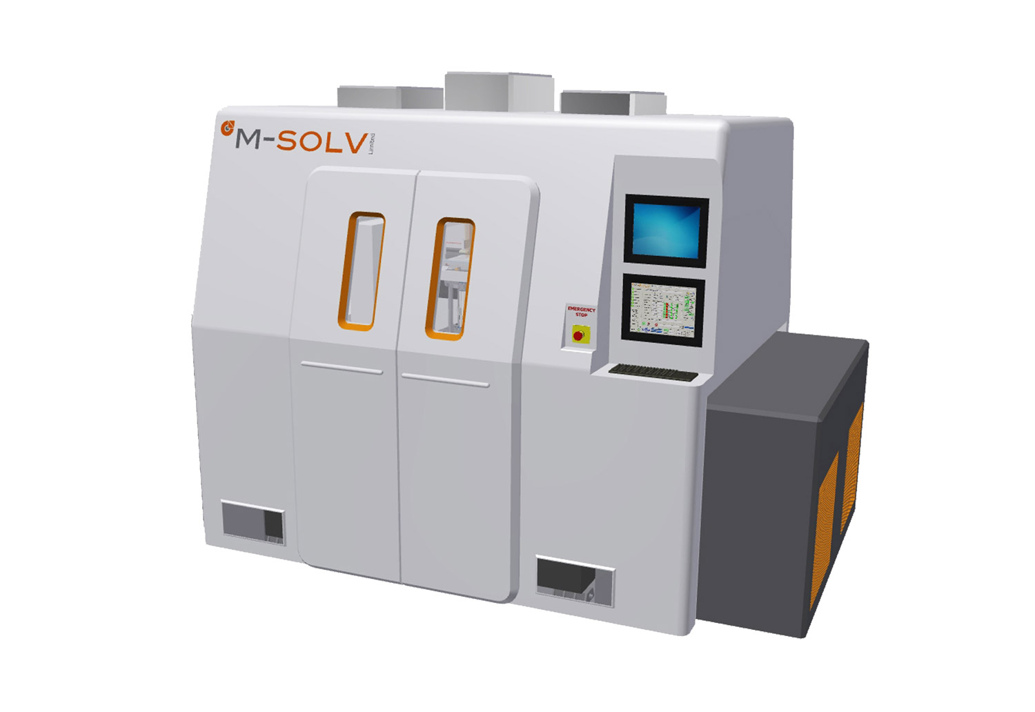
"Laser Embedded Conductor Technology" is a new process to produce smaller IC packages at low cost. First, structure widths of 1-10 µm are created by direct laser ablation of organic material. These are then filled with conductive material. This creates circuits directly on the substrate that have been defined by scanning a mask with a UV laser. At the same time, the MSV-300 system produces from M Solv the required vias. Since only solid-state lasers are used, the running costs of the laser system are comparatively low.
The MSV-600 system can process substrate sizes up to 1600x650mm, individually or from roll to roll. A wide variety of lasers, scanners and inkjet heads can be used.
The MSV 500 system is used, for example, for structuring IC substrates. Equipped with 2 lasers at 532 nm and 355 nm, conductor tracks can be written and vias can be drilled with a diameter of up to 30 µm. Up to 8 scanners can be used to process several substrates in parallel.
M-Solv is able to optimize its systems for specific processes. The plant concept permits many modifications.


