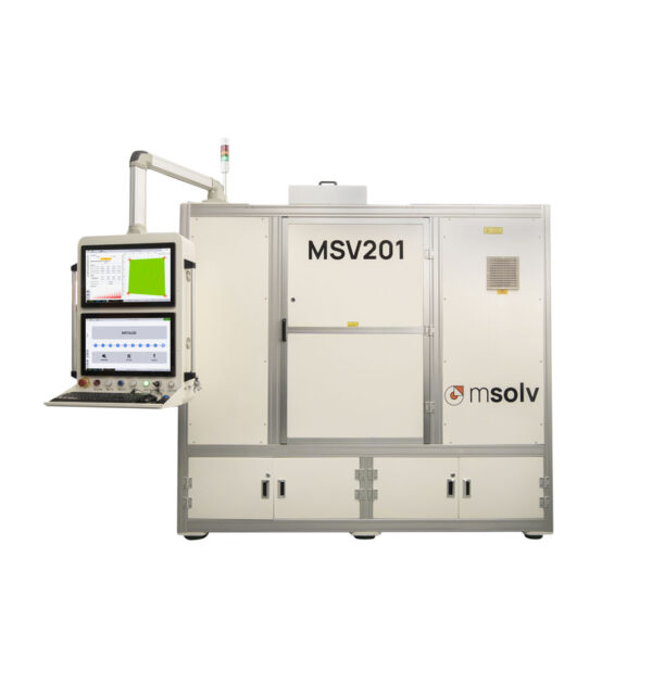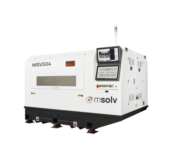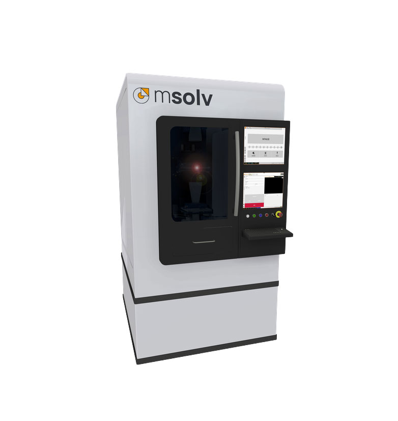
MSV300 – High-Resolution Laser Structuring for Advanced Packaging
The MSV300 by msolv is a high-precision laser processing system for the Laser Direct Ablation (LDA) of organic IC substrates. The platform was specifically developed for the next generation of highly integrated IC substrates and interposers, enabling the precise patterning of traces and vias for modern Fan-out and advanced packaging processes.
The system specifically addresses structural sizes in the range of approximately 1 to 10 µm, in which conventional manufacturing processes either reach their resolution limits or are associated with high process costs. Conductor paths and vias can be structured using a novel laser-based process.
Scanned Mask Imaging (SMI)
The core of the MSV300 is the proprietary Scanned Mask Imaging (SMI)-Technology by msolv. Unlike traditional direct-write methods, the pattern is transferred to the substrate using a mask. As a result, the process speed is largely independent of the pattern density.
A special advantage of SMI is the selective control of the ablation depth. The width and depth of conductor track structures can be varied in a targeted manner, allowing three-dimensional structures to be created directly in the substrate – without the use of multiple exposure steps or complex chemical processes.
Embedded Conductor Patterning
A central application of the MSV300 is the manufacture embedded conductor structures. In the process, printed conductors are embedded directly into the surface of organic substrates and subsequently metallized. With its SMI technology, Msolv cites structures down to 5/5 µm Lines/Spaces.
The embedded structuring enables a higher packaging density and shorter electrical connection paths. At the same time, surface planarity can be improved and the number of required routing or ground layers reduced. This makes it possible to realize thinner and more compact IC packages.
Precise structuring of organic substrates
The MSV300 is specifically designed for modern organic substrate materials and high-resolution packaging applications. The high registration accuracy enables small via-to-pad ratios, thereby supporting the increasing miniaturization of electronic assemblies.
The technology is therefore particularly suitable for applications where classical lithography or conventional laser direct write methods reach their limits in terms of resolution, process complexity, or cost.
Typical applications
- IC substrate and interposer
- Advanced Semiconductor Packaging
- Fan-Out Wafer and Panel Level Packaging
- Embedded Conductor Patterning
- High-resolution conductive trace structures
- Laser structuring of vias
- 3D structuring of organic substrates
- Next-Generation Electronic Packaging
MSV300 by msolv
With the MSV300 and the Scanned Mask Imaging technology Does MKS/MSolv offer a specialized platform for high-resolution laser structuring in the modern semiconductor and packaging industry? The combination of mask-based processing, selective depth control, and high registration accuracy enables complex structures combined with an efficient process flow.
Soliton assists you in evaluating and configuring the MSV300 for your application in IC substrates, interposers, and advanced packaging.