P2 and P3 processing of CIGS with laser precision (CIGS laser processing)
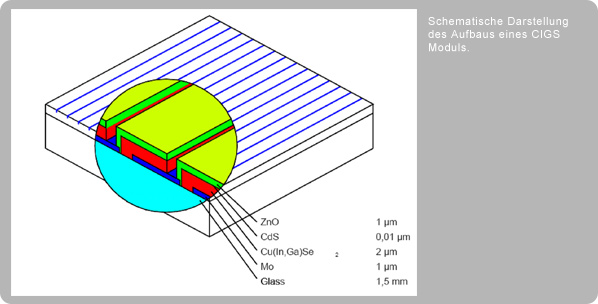
The production of thin-film photovoltaic modules requires a precise combination of coating and ablation processes. Different materials are applied to a glass plate in layers and then removed in a targeted manner to form the individual solar cells. These consist of two electrodes (top and bottom) and a photovoltaic layer in the middle. CIGS laser processing plays a central role here.

Structure of CIGS cells and the importance of P-ablation processes
CIGS cells (copper indium gallium diselenide) are usually manufactured on a molybdenum (Mo) electrode layer. Three central ablation processes are required for precise production:
- P1: Ablation of the molybdenum layer on the glass
- P2: Removal of the CIGS layer on the molybdenum
- P3: Removal of the transparent electrode layer together with the CIGS layer on the molybdenum
These steps are crucial to ensure the electrical insulation and functionality of the solar cells. While the P1 process is traditionally carried out with ns laser pulses, P2 and P3 are often carried out mechanically by scratching with needles. However, this process leads to rapid wear of the needles, which affects the process stability and efficiency.
Laser as a solution for P2 and P3
A new fiber laser from ESI-Pyrophotonics offers a programmable pulse duration and pulse shape in the range of 2 to 250 ns, with an impressive resolution of 1 ns. This enables the laser to perform the processes P2 and P3 precisely and without mechanical wear. These properties actively contribute to the CIGS laser processing to significantly optimize and at the same time increase production efficiency.
Investigations at Pyrophotonics, NRC Canada and the National Center for Photovoltaics also show that 1064 nm pulses with a pulse duration of 5 to 10 ns deliver particularly reliable results. These short pulses prevent thermal melting and thus actively minimize undesirable effects such as short circuits or material build-up that could affect the quality of the modules.
The mechanism of laser-induced ablation
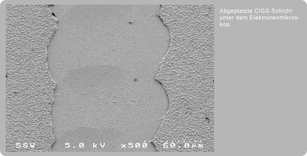
In contrast to thermal ablation, the removal in P2 and P3 processing is based on a laser-induced blasting the CIGS layer. The laser light with a wavelength of 1064 nm penetrates through the CIGS layer and is absorbed at the interface with the molybdenum layer. This process generates gas pressure through the release of selenium (Se) gas, which detaches the CIGS layer. This mechanism is particularly effective in CIGS laser processing.
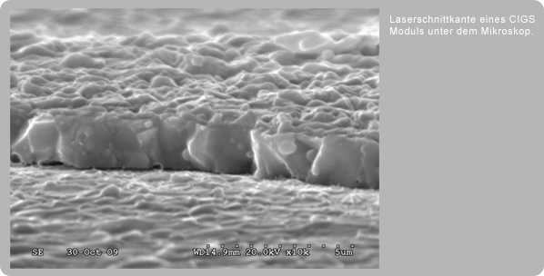
This mechanism creates a clean fracture edge, as electron micrographs show. No melting occurs, which minimizes the risk of short circuits.


Analysis and process optimization in CIGS laser processing
With EDX images (Energy Dispersive X-ray Spectroscopy) revealed that only minimal residues of copper, indium and gallium remain at the bottom of the machined track. Selenium, however, is present throughout the track, confirming the removal mechanism described.
Another advantage is the wide process window. With correctly set pulse duration, the energy density and focus depth are large enough to ensure a stable and industrially reliable processing process. This proves the value of CIGS laser processing.

Advantages
The use of a fiber laser in the processing of CIGS photovoltaic modules offers numerous advantages:
- Higher precision: Avoid thermal damage and produce cleaner cutting edges.
- Increased efficiency: Elimination of mechanical wear of needles.
- Flexibility: Adjustable pulse duration and pulse shape for different requirements.
- Stability: A large process window guarantees reliable processing.
- Reduced production costs: Fewer failures and lower maintenance costs.
Applications and Future Perspectives of CIGS Laser Processing
Laser-based P2 and P3 processing opens up new possibilities for the production of efficient and cost-effective photovoltaic modules. In addition to CIGS processing, similar processes could also be used for other thin-film technologies such as CdTe or perovskite solar cells.
Through continuous improvements in laser technology – especially in pulse shaping and energy efficiency – the Laser Stereolithography increasingly the preferred method for precision processes in the photovoltaic industry.
